|
The laboratory was established in 2010 by Dr. Tomasz Słupiński (1962-2024) and Dr. Wojciech Pacuski as part of the Center for Preclinical Research and Technology (CePT) at the Solid State Physics Division, Institute of Experimental Physics, Faculty of Physics, University of Warsaw. Since 2014, the laboratory has been housed in Cent I building (room 1.222).
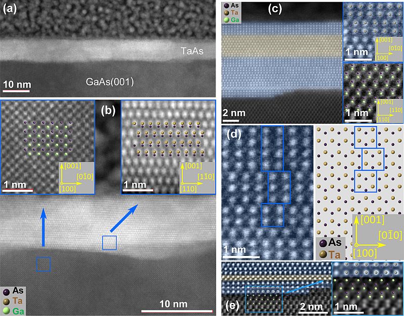
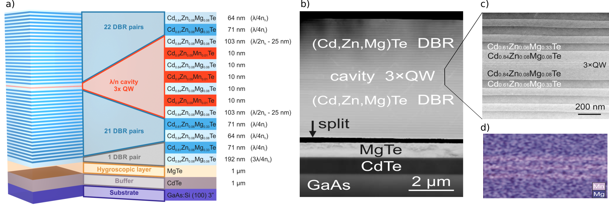
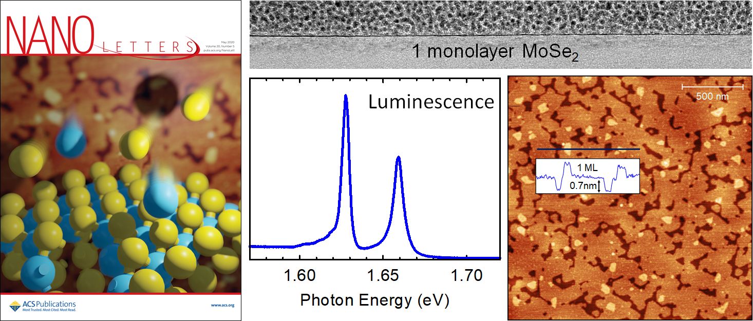
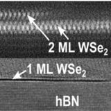
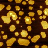
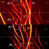
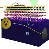
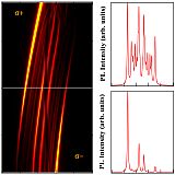
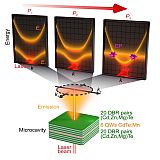
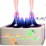
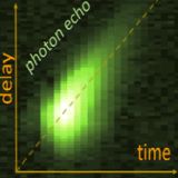
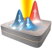
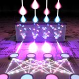
Among our achievements is a recipe for growth of high optical quality TMD monolayers using hBN substrate [51,58,69], the first epitaxial growth of topological semimetals TaAs [65,74] and NiTe2 [57], the first observation of a QD with a single Co ion [16,35] and with a single Fe ion [26,32], and farbication of semimagnetic microcavites with amazing magnetooptical properties [7,15,20,27,34,37,39,43,53,55,56,62,64,67,71,73]. The list of our publications (almost 100) is provided below. Below there are also graphics produced to advertise our research.

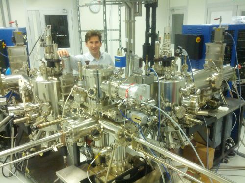
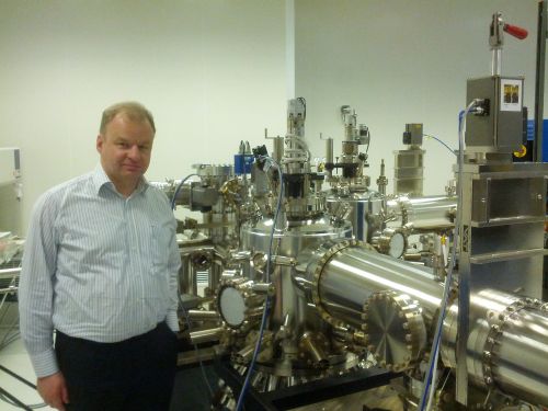
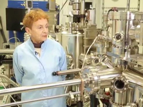
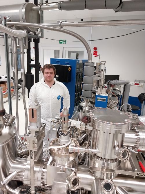
Wojciech Pacuski
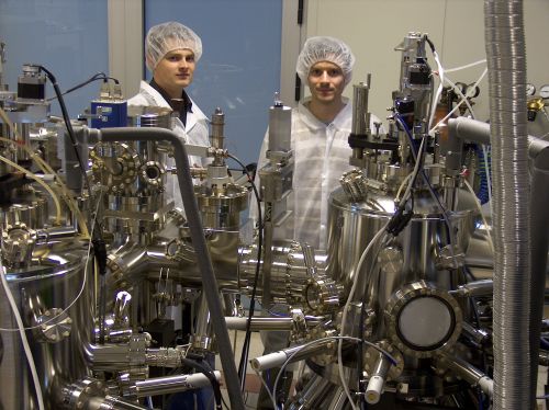
Adam Szczerba
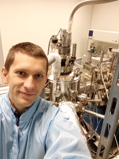
Selfie from our MBE lab 2020:
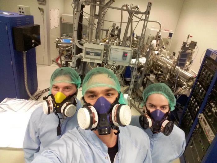
Wojciech Pacuski, Bartłomiej Seredyński, Karolina Połczyńska
Celebration of sample UW1000:
Year 2018, we are celebrating sample UW1000 together with colleagues from LUMS
group.
Publications based on samples grown in our MBE lab:
 |
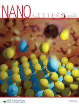
98. "WSe2 Monolayers Grown by Molecular Beam Epitaxy on hBN",
J. Kucharek, M. Raczynski, R. Bozek, A. Kaleta, B. Kurowska, M. Bilska, S. Kret, T. Taniguchi, K. Watanabe, P. Kossacki, M. Goryca, W. Pacuski,
Nano Letters 25, 17275 (2025).


|
 |
97. "Magnetic field induced polarization enhancement in the photoluminescence of MBE-grown WSe2 layers",
M. C. Kuna, M. Raczyński, J. Kucharek, T. Taniguchi, K. Watanabe, T. Kazimierczuk, W. Pacuski, P. Kossacki,
Solid State
Commun. 409, 116263 (2026).
|
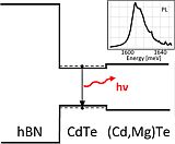
96. "Hole to Electron Crossover in a (Cd,Mn)Te Quantum Well through Surface Metallization",
A. Dydniański, M. Raczyński, A. Łopion, T. Kazimierczuk, J. Kasprzak, K. E. Połczyńska, W. Pacuski, P. Kossacki,
ArXiv:2512.04631 (2025).
|
95. "Multiplexed back focal plane imaging with on-chip integrated microlens array",
M. Furman, M. Muszyński, P. Oliwa, Ł. Zinkiewicz, A. Bogucki, J. Szczytko, P. Wasylczyk, W. Pacuski, M. Król, B. Piętka,
ArXiv:2510.09348 (2025).
|
94. "Optical and structural properties of Zn1-xMgxTe epitaxial layers grown by molecular beam epitaxy",
D. Singh, P. K. Singh, W. Pacuski, K. Strzałkowski, A. Abouais, G. Trykowski,
Available at SSRN (2025).

|
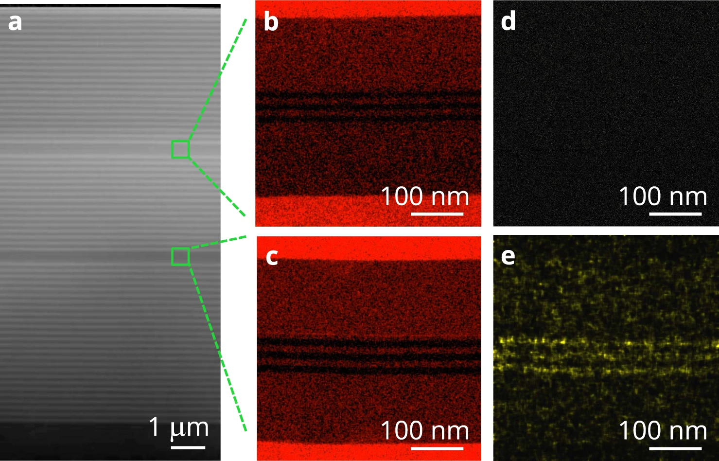
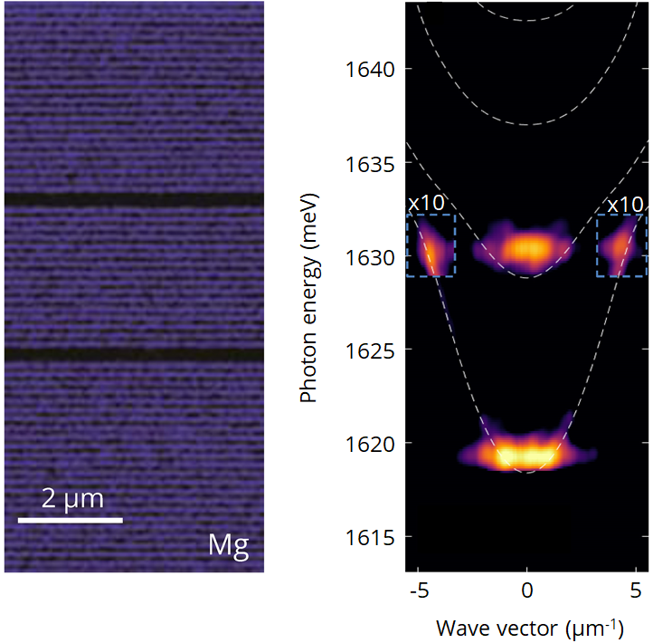
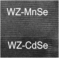
93. "Wurtzite MnSe as a barrier for CdSe quantum wells with built-in electric field",
M. J. Grzybowski, W. Pacuski, J. Suffczyński,
ArXiv:2508.17899 (2025).
|
92. "Optical bound states in the continuum in subwavelength gratings made of an epitaxial van der Waals material",
E. Pruszyńska-Karbownik, T. Fąs, K. Brańko, D. Yavorskiy, B. Stonio, R. Bożek, P. Karbownik, J. Wróbel, T. Czyszanowski, T. Stefaniuk, W. Pacuski, J. Suffczyński,
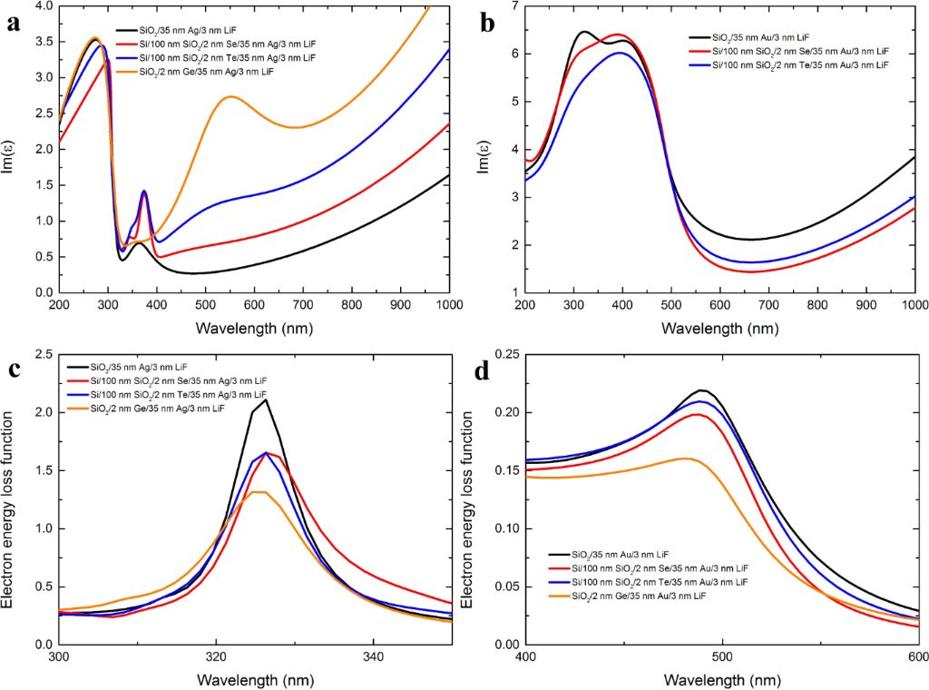
ArXiv:2502.03121 (2025).
|
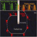 |
91. "Emission enhanced exciton-polariton condensates with optical feedback",
R. Mirek, M. Furman, A. Opala, M. Król, W. Pacuski, J. Szczytko, H. Sigurðsson, B. Piętka,
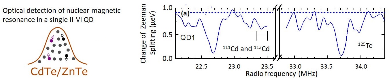
ACS Photonics in press (2025).
|
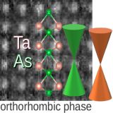 |
90. "Orthorhombic TaAs: A New Topological Phase of the Archetypical Weyl Semimetal",
Z. Ogorzałek, C.-C. Lee, J. Z. Domagala, W. Zajkowska-Pietrzak, S. Kret, R. BożekW. Pacuski, I. Lutsyk, W. Ryś, P. J. Kowalczyk, M. Tokarczyk, M. Polakowski, D. Wasik, J. Sadowski, B.-H. Huang, H. Lin, M. Gryglas-Borysiewicz,
ACS Applied Materials & Interfaces 17, 51386 (2025).
|
 |
89. "Photoluminescence efficiency of MBE-grown MoSe2 monolayers featuring sharp excitonic lines and diverse grain structures",
M. Raczyński, J. Kucharek, K. Oreszczuk, A. Rodek, T. Kazimierczuk, R. Bożek, T. Taniguchi, K. Watanabe, W. Pacuski, P. Kossacki,
Journal of Luminescence 288, 121576 (2025).
|
 |
88. "Influence of local strain on the optical probing of a Ni spin in a charged self-assembled quantum dot",
K. E. Polczynska, S. Karouaz, W. Pacuski, L. Besombes,
Phys. Rev. B 112, 245301 (2025).
|
 |
87. "Strain-induced speed-up of Mn2+ spin-lattice relaxation in (Cd,Mn)Te/(Cd,Mg)Te quantum wells: a time-resolved ODMR study",
A. Bogucki, A. Łopion, K. E. Połczyńska, W. Pacuski, T. Kazimierczuk, A. Golnik, P. Kossacki,
Phys. Rev. B 112, 035407 (2025).
|
 |
86. "The Integration of Raman Spectrometer with Glove Box for High-Purity Investigation in an Inert Gas Condition",
M. Piskorski, I. Lutsyk, W. Ryś, M. Le Ster, Z. Ogorzałek-Sory, K. Toczek, A. Nadolska, R. Dunal, P. Przybysz, M. Rogala, P. Dąbrowski, W. Pacuski, J. Sadowski, M. Gryglas-Borysiewicz, P. J. Kowalczyk, W. Kozłowski, P. Krukowski,
Measurement 251, 117190 (2025).
|
 |
85. "The single ion of Vanadium in an individual Quantum Dot ",
K. E. Połczyńska, T. Kazimierczuk, P. Kossacki, W. Pacuski,
Phys. Rev. B 111, 085428 (2025).

|
 |
84. "Impact of the Hole Gas on Optically Detected Magnetic Resonance in (Cd,Mn)Te Based Quantum Well",
A. Łopion, A. Bogucki, M. Raczyński, Z. Śnioch, K. E. Połczyńska, W. Pacuski, T. Kazimierczuk, A. Golnik, P. Kossacki,
Phys. Rev. B 111, 035307 (2025).

|
 |
83. "Spin-lattice relaxation of (Cd,Mn)Te co-doped with Co ions",
A. Łopion, K. Oreszczuk, A. Bogucki, K.E. Połczyńska, W. Pacuski, T. Kazimierczuk, A. Golnik, P. Kossacki,
Solid State Commun. 396, 115753 (2025).
|
 |
82. "Carrier localization in defected areas of (Cd, Mn)Te quantum well investigated via Optically Detected Magnetic Resonance employed in the microscale",
A. Dydniański, A. Łopion, M. Raczyński, T. Kazimierczuk, K.E. Połczyńska, W. Pacuski, P. Kossacki,
Solid State Commun. 396, 115755 (2025).
|
 |
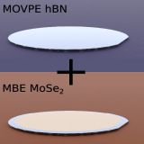
81. "Large-Area Growth of High-Optical-Quality MoSe2/hBN Heterostructures with Tunable Charge Carrier Concentration",
K. Ludwiczak, A. K. Dąbrowska, J. Kucharek, J. Rogoża, M. Tokarczyk, R. Bożek, M. Gryglas-Borysiewicz, T. Taniguchi, K. Watanabe, J. Binder, W. Pacuski, A. Wysmołek,,
ACS Appl. Mater. Interfaces 16, 49701(2024).
|
 |
80."Device implementing polariton optical neural network and polariton optical neural network",
M. Matuszewski, B. Pietka, A. Opala, J. Szczytko, R. Mirek, K. Tyszka, M. Król, M. Furman, J. Suffczyński, W. Pacuski, B. Seredyński,
US Patent US20240143990A1 (2024).
|
 |
79. "Optical probing of the carriers-mediated coupling of the spin of two Co atoms in a quantum dot",
L. Besombes, J. Kobak, W. Pacuski,
Phys. Rev. B 109, 235302 (2024).
|
 |
78. "Short excitonic lifetimes of MoSe2 monolayers grown by molecular beam epitaxy on the hexagonal boron nitride",
K. Oreszczuk, W. Pacuski, A. J. Rodek, M. Raczynski, T. Kazimierczuk, K. Nogajewski, T. Taniguchi, K. Watanabe, M. Potemski, Piotr Kossacki,
2D Materials 11, 025029 (2024).
|
 |
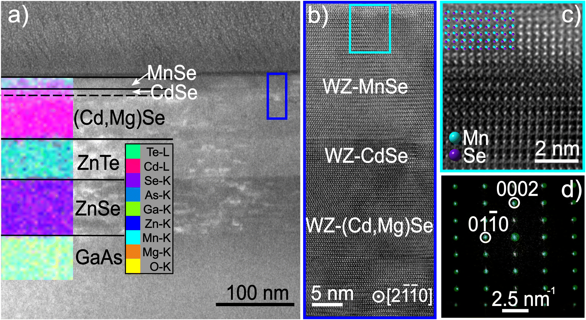
77. "Wurtzite vs rock-salt MnSe epitaxy: electronic and altermagnetic properties",
M. J. Grzybowski, C. Autieri, J. Domagała, C. Krasucki, A. Kaleta, S. Kret, K. Gas, M. Sawicki, R. Bożek, J. Suffczyński, W. Pacuski,
Nanoscale 16, 6259 (2024).
|
 |
76. "Raman scattering excitation in monolayers of semiconducting transition metal dichalcogenides",
M. Zinkiewicz, M. Grzeszczyk, T. Kazimierczuk, M. Bartos, K. Nogajewski, W. Pacuski, K. Watanabe, T. Taniguchi, A. Wysmołek, P. Kossacki, M. Potemski, A. Babiński, M. R. Molas,
npj 2D Materials and Applications 8, 2 (2024) .
(Paper is mainly on exfoliated 2D materials, data on MBE samples are in SI)
|
 |
75. "Molecular beam epitaxy growth of cadmium telluride structures on hexagonal boron nitride",
A. K. Szczerba, J. Kucharek, J. Pawłowski, T. Taniguchi, K. Watanabe, W. Pacuski,
ACS Omega 8, 44745 (2023).
|
 |
73. "Universality of open microcavities for stronglight-matter coupling",
M. Król, K. Lempicka, K. Rechcinska, M. Furman, K. Nogajewski, R. Mazur, P. Morawiak, W. Piecek, W. Pacuski, J. Szczytko, B. Pietka,
Optical Materials Express 13, 2651(2023).
|
 |
72. "Natural exceptional points in the excitation spectrum of a light-matter system",
A. Opala, M. Furman, M. Król, R. Mirek, K. Tyszka, B. Seredyński, W. Pacuski, J. Szczytko, M. Matuszewski, B. Piętka,
Optica 10, 1111 (2023).
|
 |
71. "Magneto-optical induced supermode switching in quantum fluids of light",
M. Furman, R. Mirek, M. Król, W. Pacuski, H. Sigurðsson, J. Szczytko, B. Piętka,
Communications Physics 6, 196 (2023).
|
 |
69. "Coherent imaging and dynamics of excitons in MoSe2 monolayers epitaxially grown on hexagonal boron nitride",
K. E. Połczyńska, S. Le Denmat, T. Taniguchi, K. Watanabe, M. Potemski, P. Kossacki, W. Pacuski, J. Kasprzak,
Nanoscale 15, 6941 (2023).
,
|
 |
68. "Inverted optical bistability and optical limiting in coherently driven exciton–polaritons",
M. Furman, A. Opala, M. Król, K. Tyszka, R. Mirek, M. Muszyński, B. Seredyński, W. Pacuski, J. Szczytko, M. Matuszewski, B. Piętka,
APL Photonics 8, 046105 (2023).
Supplemental information.
|
 |
67. "Spin polarization of exciton-polariton condensate in a photonic synthetic effective magnetic field",
R. Mirek, M. Furman, M. Król, B. Seredyński, K. Łempicka-Mirek, K. Tyszka, W. Pacuski, M. Matuszewski, J. Szczytko, B. Piętka,
Phys. Rev. B 107, 125303 (2023).
|
 |
66. "Magnetic ion relaxation time distribution within a quantum well",
A. Łopion, A. Bogucki, W. Kraśnicki, K. E. Połczyńska, W. Pacuski, T. Kazimierczuk, A. Golnik, P. Kossacki,
Phys. Rev. B 106, 165309 (2022).
|
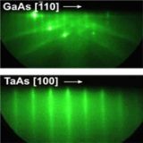 |
65. "Structural properties of TaAs Weyl semimetal thin films grown by molecular beam epitaxy on GaAs(001) substrates",
J. Sadowski, J. Z. Domagała, W. Zajkowska, S. Kret, B. Seredyński, M. Gryglas-Borysiewicz, Z. Ogorzałek, R. Bożek, W. Pacuski,
Cryst. Growth Des. 22, 6039 (2022).
|
 |
64. "Neural networks based on ultrafast time-delayed effects in exciton-polaritons",
R. Mirek, A. Opala, M. Furman, M. Król, K. Tyszka, B. Seredyński, W. Pacuski, J. Suffczyński, J. Szczytko, M. Matuszewski, B. Piętka,
Phys. Rev. Applied 17, 054037 (2022).
|
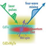 |
63. "Coherent dynamics of a single Mn-doped quantum dot revealed by four-wave mixing spectroscopy",
J. Kasprzak, D. Wigger, T. Hahn, T. Jakubczyk, Ł. Zinkiewicz, P. Machnikowski, T. Kuhn, J.-F. Motte, W. Pacuski,
ACS Photonics 9, 1033–1041 (2022).
,
Supporting Information.
|
 |
62. "Leaky Integrate-and-Fire Mechanism in Exciton-Polariton Condensates for Photonic Spiking Neurons",
K. Tyszka, M. Furman, R. Mirek, M. Król, A. Opala, B. Seredyński, J. Suffczyński, W. Pacuski, M. Matuszewski, J. Szczytko, B. Piętka,
Laser Photonics Rev. 2100660 (2022).
Supporting Information.
|
 |
60. "Angle-resolved optically detected magnetic resonance as a tool for strain determination in nanostructures",
A. Bogucki, M. Goryca, A. Łopion, W. Pacuski, K. Połczyńska, J. Domagała, M. Tokarczyk, T. Fąs, A. Golnik, P. Kossacki,
Phys. Rev. B (2021).
|
 |
59. "Impact of Stripe Shape on the Reflectivity of Monolithic High Contrast Gratings",
M. Marciniak, T.-S. Chang, T.-C. Lu, F. Hjort, A. Haglund, Ł. Marona, M. Gramala, P. Modrzyński, R. Kudrawiec, K. Sawicki, R. Bożek, W. Pacuski, J. Suffczyński, M. Gębski, A. Broda, J. Muszalski, J. A. Lott, T. Czyszanowski,
ACS Photonics 8, 3173(2021).
|
 |
58. "Heteroepitaxial growth of high optical quality, wafer-scale van der Waals heterostrucutres",
K. Ludwiczak, A. K. Dąbrowska, J. Binder, M. Tokarczyk, J. Iwański, B. Kurowska, J. Turczyński, G. Kowalski, R. Bożek, R. Stępniewski, W. Pacuski, A.Wysmołek,
ACS Appl. Mater. Interfaces 13, 47904 (2021).
|
 |
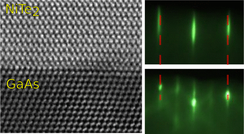
57. "Molecular Beam Epitaxy of a 2D Material Nearly Lattice Matched to a 3D Substrate: NiTe2 on GaAs",
B. Seredyński, Z. Ogorzałek, W. Zajkowska, R. Bożek, M. Tokarczyk, J. Suffczyński, S. Kret, J. Sadowski, M. Gryglas-Borysiewicz, W. Pacuski,
Cryst. Growth Des. 21, 5773 (2021).
|
 |
55. "Neuromorphic binarized polariton networks",
R. Mirek, A. Opala, P. Comaron, M. Furman, M. Król, K. Tyszka, B.j Seredyński, D. Ballarini, D. Sanvitto, T. C. H. Liew, W. Pacuski, J. Suffczyński, J. Szczytko, M. Matuszewski, B.Piętka,
Nano Letters 21, 3715 (2021).
Supporting Information,
Press release: PL.
|
 |
54. "Polariton lasing and energy-degenerate parametric scattering in non-resonantly driven coupled planar microcavities",
K. Sawicki, T. J. Sturges, M. Ściesiek, T. Kazimierczuk, K. Sobczak, A. Golnik, W. Pacuski, J. Suffczyński,
Nanophotonics 10, 2421 (2021).
Supplementary Materials,
Press release: EN,
PL.
|
| |
53. "Long-distance coupling and energy transfer between exciton states in magnetically controlled microcavities",
M. Ściesiek, K. Sawicki, W. Pacuski, K. Sobczak, T. Kazimierczuk, A. Golnik, J. Suffczyński ,
Communications Materials 1, 78 (2020).
|
 |
52. " Charge Transport in MBE-grown 2H-MoTe2 Bilayers with Enhanced Stability Provided by AlOx Capping Layer",
Z. Ogorzałek, B. Seredyński, S. Kret, A. Kwiatkowski, K. P. Korona, M. Grzeszczyk, J. Mierzejewski, D. Wasik, W. Pacuski, J. Sadowski and M. Borysiewicz,
Nanoscale 12, 16535 (2020).
|
 |
51. "Narrow excitonic lines and large-scale homogeneity of transition metal dichalcogenide monolayer grown by molecular beam epitaxy on hexagonal boron nitride",
W. Pacuski, M. Grzeszczyk, K. Nogajewski, A. Bogucki, K. Oreszczuk, J. Kucharek, K.E. Połczyńska, B. Seredyński, A. Rodek, R. Bożek, T. Taniguchi, K. Watanabe, S. Kret, J. Sadowski, T. Kazimierczuk, M. Potemski, P. Kossacki,
Nano Letters 20, 3058 (2020).
 Supporting Information,
Press release EN, PL.
Supporting Information,
Press release EN, PL.
|
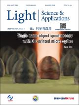 |
50. "Ultra-long-working-distance spectroscopy of single nanostructures with aspherical solid immersion microlenses",
A. Bogucki, Ł. Zinkiewicz, M. Grzeszczyk, W. Pacuski, K. Nogajewski, T. Kazimierczuk, A. Rodek, J. Suffczyński, K. Watanabe, T. Taniguchi, P. Wasylczyk, M. Potemski, P. Kossacki,
Light: Science & Applications 9, 48 (2020).
Supplementary information,
Press release EN, PL.
|
 |
49. "Direct Interbranch Relaxation of Polaritons in a Microcavity with Embedded CdSe/(Cd,Mg)Se Quantum Wells",
K. Sawicki, M. Jurczak, W. Pacuski, J. Suffczyński ,
Journal of Electronic Materials (2020).
|
 |
48. "Charged Exciton Dissociation Energy in (Cd,Mn)Te Quantum Wells with Variable Disorder and Carrier Density",
A. Łopion, A. Bogucki, K. E. Połczyńska, W. Pacuski, A. Golnik, T. Kazimierczuk, P. Kossacki,
Journal of Electronic Materials (2020).
|
 |
45. "Direct measurement of hyperfine shifts and radiofrequency manipulation of the nuclear spins in individual CdTe/ZnTe quantum dots",
G. Ragunathan, J. Kobak, G. Gillard, W. Pacuski, K. Sobczak, J. Borysiuk, M. S. Skolnick, E. A. Chekhovich,
Phys. Rev. Lett., 122, 096801 (2019).
|
 |
44. "Triple threshold lasing from a photonic trap in a Te/Se-based optical microcavity",
K. Sawicki, J.-G. Rousset, R. Rudniewski, W. Pacuski, M. Ściesiek, T. Kazimierczuk, K. Sobczak, J. Borysiuk, M. Nawrocki, J. Suffczyński
Communications Physics 2, 38 (2019).
|
 |
43. "Giant spin Meissner effect in a non-equilibrium exciton-polariton gas",
M. Król, R. Mirek, D. Stephan, K. Lekenta, J.-G. Rousset, W. Pacuski, A. V. Kavokin, M. Matuszewski, J. Szczytko, B. Piętka,
Phys Rev. B 99, 115318 (2019).
|
 |
41. "MnSe - Molecular Beam Epitaxy Growth and Optical Characterisation",
J. Kucharek, R. Bożek, W. Pacuski,
Acta Physica Polonica A 136, 598 (2019).
|
 |
40. "Interaction of Te and Se interlayers with Ag or Au nanofilms in sandwich structures",
A. Ciesielski, L. Skowronski, M. Trzcinski, E. Górecka, W. Pacuski and T. Szoplik
Beilstein J. Nanotechnol. 10, 238 (2019).
|
 |
39. "(Cd,Zn,Mg)Te-based microcavity on MgTe sacrificial buffer: Growth, lift-off, and transmission studies of polaritons",
B. Seredyński, M. Król, P. Starzyk, R. Mirek, M. Ściesiek, K. Sobczak, J. Borysiuk, D. Stephan, J.-G. Rousset, J. Szczytko, B. Piętka, W. Pacuski,
Phys. Rev. Materials 2, 043406 (2018).
|
 |
38. "Optical fiber micro-connector with nanometer positioning precision for rapid prototyping of photonic devices",
A. Bogucki, Ł. Zinkiewicz, W. Pacuski, P. Wasylczyk, P. Kossacki,
Optics Express 26, 11513 (2018).
|
 |
37. "Spin polarized semimagnetic exciton-polariton condensate in magnetic field",
M. Król, R. Mirek, K. Lekenta, J.-G. Rousset, D. Stephan, M. Nawrocki, M. Matuszewski, J. Szczytko, W. Pacuski, B. Piętka,
Scientific Reports 8, 6694 (2018).
|
 |
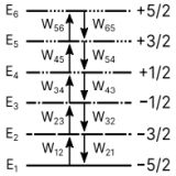
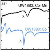
35. "Direct determination of zero-field splitting for single Co2+ ion embedded in a CdTe/ZnTe quantum dot",
J. Kobak, A. Bogucki, T. Smoleński, M. Papaj, M. Koperski, M. Potemski, P. Kossacki, A. Golnik, W. Pacuski,
Phys. Rev. B 97, 045305 (2018),
|
 |
34. "Effect of magnetic field on the lasing threshold of a semimagnetic polariton condensate",
J.-G. Rousset, B. Piętka, M. Król, R. Mirek, K. Lekenta, J. Szczytko, W. Pacuski, M. Nawrocki,
Phys. Rev. B 96, 125403 (2017) .
|
 |
33. "Origin of luminescence quenching in structures containing CdSe/ZnSe quantum dots with a few Mn2+ ions",
K. Oreszczuk, M. Goryca, W. Pacuski, T. Smoleński, M. Nawrocki, P. Kossacki,
Phys. Rev. B 96, 205436 (2017).
|
 |
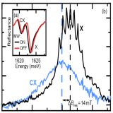
32. "Fine structure of an exciton coupled to a single Fe2+ ion in a CdSe/ZnSe quantum dot",
T. Smoleński, T. Kazimierczuk, M. Goryca, W. Pacuski, and P. Kossacki,
Phys. Rev. B 96, 155411 (2017).
|
 |
31. "Coupling of Quantum Dots with Quantum Wells in a System Based on (Cd,Zn,Mg)Te"
K. Połczyńska, E. Janik, P. Kossacki, W. Pacuski,
Acta Physica Polonica A 132, 369 (2017). |
 |
29. "Design and control of mode interaction in coupled ZnTe optical microcavities",
M. Ściesiek, W. Pacuski, J-G. Rousset, M. Parlińska-Wojtan, A. Golnik, J. Suffczyński,
Cryst. Growth Des. 17, 3716 (2017).
|
 |
28. "Antireflective photonic structure for coherent nonlinear spectroscopy of single magnetic quantum dots",
W. Pacuski, J.-G. Rousset, V. Delmonte, T. Jakubczyk, K. Sobczak, J. Borysiuk, K. Sawicki, E. Janik, J. Kasprzak,
Cryst. Growth Des. 17, 2987 (2017).
|
 |
27. "Angular dependence of giant Zeeman effect for semi-magnetic cavity polaritons",
R. Mirek, M. Król, K. Lekenta, J.-G. Rousset, M. Nawrocki, J. Szczytko, M. Kulczykowski, M. Matuszewski, W. Pacuski, B. Piętka,
Phys. Rev. B 95, 085429 (2017).
.
|
 |
25. "Effect of electron-hole separation on optical properties of individual Cd(Se,Te) quantum dots",
M. Ściesiek, J. Suffczyński, W. Pacuski, M. Parlińska-Wojtan, T. Smoleński, P. Kossacki, and A. Golnik,
Phys. Rev. B 93, 195313 (2016), or free access preprint arXiv:1603.00313.
|
 |
24. "Anisotropy of in-plane hole g factor in CdTe/ZnTe quantum dots",
A. Bogucki, T. Smoleński, M. Goryca, T. Kazimierczuk, J. Kobak, W. Pacuski, P. Wojnar, and P. Kossacki,
Phys. Rev. B 93, 235410 (2016),or free access preprint arXiv:1604.02591.
|
 |
23. "Comparison of magneto-optical properties of various excitonic complexes in CdTe and CdSe self-assembled quantum dots",
J. Kobak, T. Smoleński, M. Goryca, J.-G. Rousset, W. Pacuski, A. Bogucki, K. Oreszczuk, P. Kossacki, M. Nawrocki, A. Golnik, J. Płachta, P. Wojnar, C. Kruse, D. Hommel, M. Potemski, T. Kazimierczuk,
J. Phys.: Condens. Matter 28, 265302 (2016)or free access preprint http://arxiv.org/abs/1602.06118
|
 |
22. "Distributed Bragg reflectors obtained by combining Se and Te compounds: Influence on the luminescence from CdTe quantum dots",
J.-G. Rousset, J. Kobak, E. Janik, M. Parlinska-Wojtan, T. Slupinski, A. Golnik, P. Kossacki, M. Nawrocki, W. Pacuski,
J. Appl. Phys. 119, 183105 (2016). |
 |
21. "Epitaxial growth and Photoluminescence Excitation spectroscopy of CdSe Quantum Dots in (Zn,Cd)Se barrier",
J. Piwowar, W. Pacuski, T. Smoleński, M. Goryca, A. Bogucki, A. Golnik, M. Nawrocki, P. Kossacki, J. Suffczyński,
Journal of Luminescence 173, 94 (2016),or free access preprint arXiv:1512.07929.
|

|
20. "Strong coupling and polariton lasing in Te based microcavities embedding (Cd,Zn)Te quantum wells",
J.-G. Rousset, B. Piętka, M. Król, R. Mirek, K. Lekenta, J. Szczytko, J. Borysiuk, J. Suffczyński, T. Kazimierczuk, M. Goryca, T. Smoleński, P. Kossacki, M. Nawrocki, W. Pacuski.
Applied Physics Letters 107, 201109 (2015), or free access preprint
arXiv:1510.04723
|

|
18. "Single-color, in situ photolithography marking of individual CdTe/ZnTe quantum dots containing a single Mn2+ ion",
K. Sawicki, F. K. Malinowski, K. Gałkowski, T. Jakubczyk, P. Kossacki, W. Pacuski, J. Suffczyński,
Appl. Phys. Lett. 106, 012101 (2015).
|
 |
16. "Designing quantum dots for solotronics"
J. Kobak, T. Smoleński, M. Goryca, M. Papaj, K. Gietka, A. Bogucki, M. Koperski, J.-G. Rousset, J. Suffczyński, E. Janik, M. Nawrocki, A. Golnik, P. Kossacki, W. Pacuski,
Nature Communications 5, 3191 (2014).
Supplementary Information.
Press release: EN,
PL.
|
 |
15. " MBE grown microcavities based on selenium and tellurium compounds",
J.-G. Rousset, J. Kobak, E. Janik, T. Jakubczyk, R. Rudniewski, P. Piotrowski, M. Ściesiek, J. Borysiuk, T. Slupinski, A. Golnik, P. Kossacki, M. Nawrocki, W. Pacuski,
Journal of Crystal Growth 401, 499 (2014). |
14. "The impact of position of Mn delta-doping on the formation of CdTe/ZnTe quantum dots with single magnetic ions",
K. Gietka, J. Kobak, E. Janik, J.G. Rousset, J. Borysiuk, M. Nawrocki, A. Golnik, P. Kossacki, W. Pacuski,
Journal of Crystal Growth 401, 640 (2014).
13. "Photoluminescence studies of giant Zeeman effect in MBE-grown cobalt-based dilute magnetic semiconductors",
M. Papaj, J. Kobak, J.G. Rousset, E. Janik, M. Nawrocki, P. Kossacki, A. Golnik, W. Pacuski,
Journal of Crystal Growth 401, 644 (2014).
|
11. "Photoluminescence Dynamics of CdSe Quantum Dot with Single Mn2+ Ion Under Modulated Excitation"
M. Pilat , M. Goryca, T. Smoleński, W. Pacuski, P. Kossacki,
Acta Physica Polonica A 126, 1212 (2014).
10. "Type I CdSe and CdMgSe Quantum Wells"
R. Rudniewski, J.-G. Rousset, E. Janik, P. Kossacki, A. Golnik, M. Nawrocki, W. Pacuski,
Acta Physica Polonica A 126, 1167 (2014).
9. "Optical Properties of CdTe QDs in Proximity to a Surface"
J. Piwowar, J. Papierska, K. Sawicki, J. Kobak, W. Pacuski, A. Golnik, P. Kossacki, J. Suffczyński,
Acta Physica Polonica A 124, 795 (2013).
|
 |
8. "Ultra low density of CdTe quantum dots grown by MBE",
J. Kobak, J.-G. Rousset, R. Rudniewski, E. Janik, T. Słupiński, P. Kossacki, A. Golnik, W. Pacuski,
Journal of Crystal Growth 378, 274 (2013). |
 |
7. "MBE growth and characterization of a II-VI distributed Bragg reflector and microcavity lattice-matched to MgTe",
J.-G. Rousset, J. Kobak, T. Slupinski, T. Jakubczyk, P. Stawicki, E. Janik, M. Tokarczyk, G. Kowalski, M. Nawrocki, W. Pacuski,
Journal of Crystal Growth 378, 266 (2013). |
 |
6. "MBE Growth of CdTe/ZnTe Quantum Dots with Single Mn Ions",
K. Gietka, J. Kobak, J.-G. Rousset, E. Janik, T. Słupiński, P. Kossacki, A. Golnik, W. Pacuski,
Acta Physica Polonica A 122, 1056 (2012). |
5. "MBE Growth and Magnetooptical Properties of (Zn,Co)Te Layers",
M. Papaj, J. Kobak, J.-G. Rousset, E. Janik, A. Golnik, P. Kossacki, W. Pacuski,
Acta Physica Polonica A 122, 1010 (2012).
|
 |
4. "MBE Growth and Characterization of a III-V Distributed Bragg Reflectors and InAs Quantum Dots"
J.-G. Rousset, T. Słupinski, T. Jakubczyk, J. Kobak, P. Stawicki, K. Gołasa, A. Babinski, M. Nawrocki, W. Pacuski,
Acta Physica Polonica A 122, 984 (2012). |
2. "Efficient Emission from InAlGaAs Single Quantum Dots with Low Lattice Misfit and AlGaAs Indirect Bandgap Barrier",
T. Słupiński, K.P. Korona, J. Papierska, J. Borysiuk,
Acta Physica Polonica A 130, 1229 (2016).
|
1. "Donor-deactivating defects above the equilibrium doping limit in GaAs:Te,Ge and GaAs:Te studied by annealing and Hall effect under pressure",
T. Slupinski, D. Wasik, J. Przybytek,
Journal of Crystal Growth 468, 433 (2017).
|
We are open to scientific cooperation.
Visit home page of dr hab. Wojciech Pacuski
We are excited that dr. Michał Grzybowski starts realization of his own project in our lab.
We started growth on September 29, 2011.
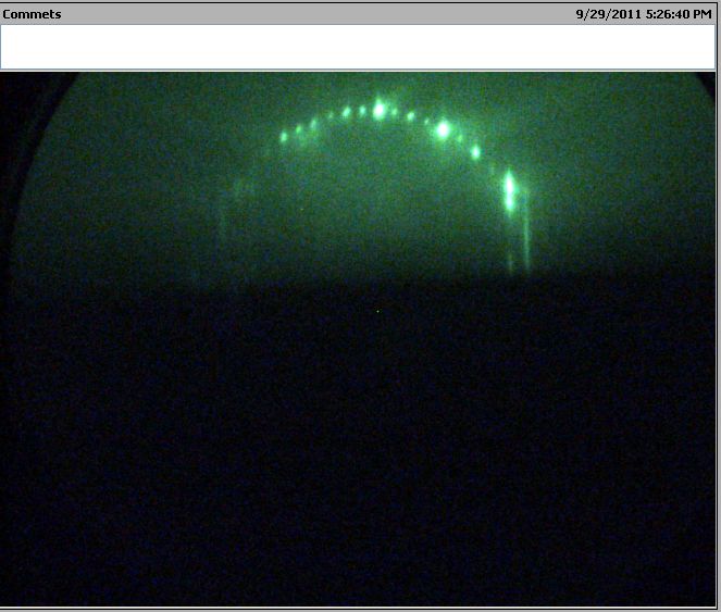
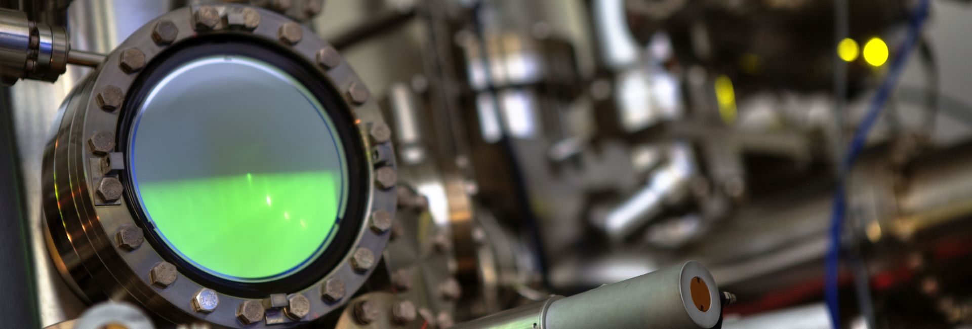
RHEED image of our first layer, GaAs on GaAs substrate.
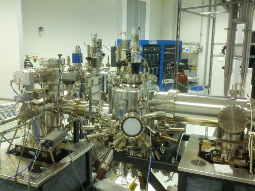
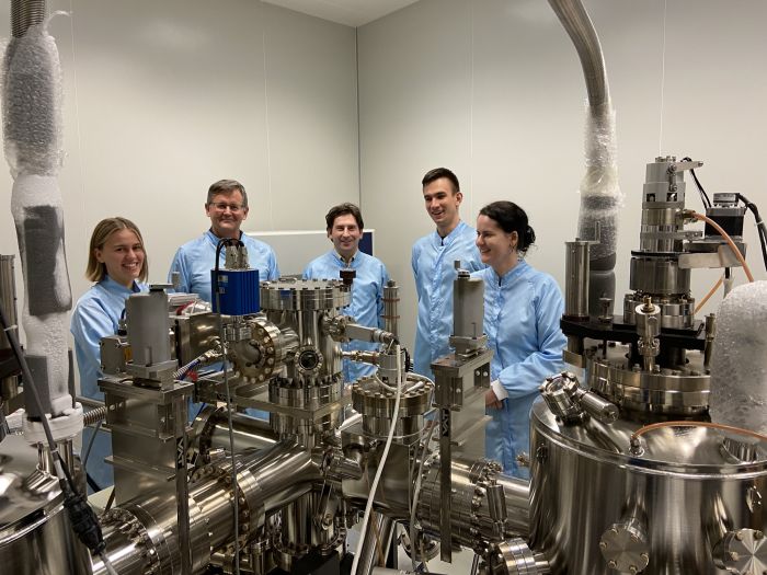
Our MBE in a new cleanroom, 2014.
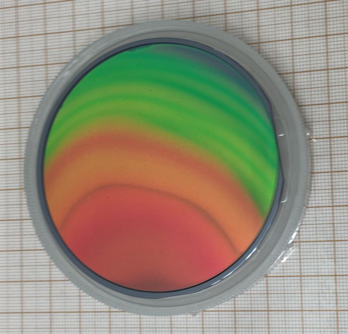
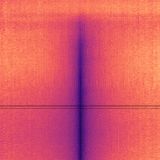
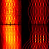
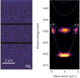
Example of microcavity sample grown in March, 2018
Our Team 2011-2017:
|