My field of interest is a solid state physics; mainly, optical and electrical properties of III-V semiconductors.
I investigate luminescence, photosensitivity and conductivity of these materials. This materials can be use to produce UV AlGaInN detectors and emmiters. In my lab in Institute of Experimental Physics I can measure time-resolved spectroscopy, using a streak-camera. I have built a set-up for measurements of low currents. This setup is well prepared for measurements of photo-current, thermally stimulated current TSC, and photo-induced current-transient spectroscopy (PICTS).
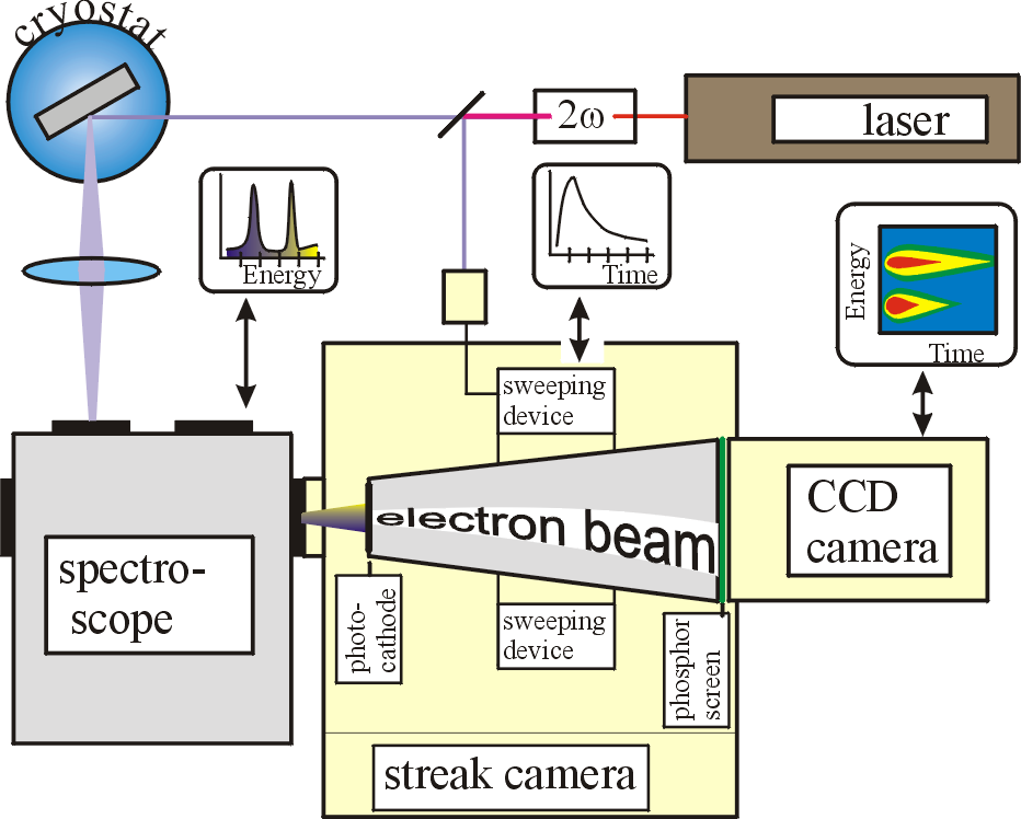
Equipment for measurements of time-resolved photoluminescence (TRPL)
with a streak camera.
 |
 Luminescence streaks of a GaInN/GaN quantum well. |
In this experimental technique a laser pulse excites a sample in a cryostat. The photoluminescence signal from the sample is first dispersed in a spectroscope (spectral-resolution) and then fed into a streak camera for temporal resolution. In the streak camera the light beam is converted to electron beam, which goes through a sweeping device where it is swept like in oscilloscope. Finally the obtained signal is spectrally- and time- resolved. The advantage of this method is the simultaneous recording of many transients at the same time, which gives a possibility of reliable comparison of various processes.
Examples of streak-camera images (measured in Faculty of Physics, University of Warsaw).
.gif) |
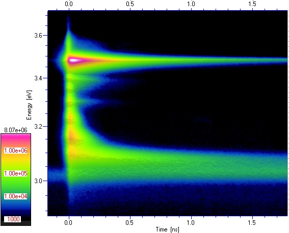
TRPL of a GaInN/GaN quantum well on GaN. GaN barrier emits at about 3.46 eV. The QW PL is at 3.05 eV. The sample was used for investigation of dynamics of cooling and recombination of excitons in a QW. Details in: For details see: J. Binder, K. P. Korona, A. Wysmołek, M. Kamińska, K. Köhler, L. Kirste, O. Ambacher, M. Zajac, R. Dwiliński, "Dynamics of Thermalization within a GaInN/GaN QWs Grown on Ammonothermal GaN" , J. Appl. Phys. 114, 223504 (2013) , DOI: 10.1063/1.4845715 |
 |
TRPL of InAlGaAs single quantum dots. Time-resolved micro-photoluminescence was measurements on In0.40Al0.45Ga0.15As single QDs. Wide band of photoluminescence from background dots as well as sharp peaks from single QDs with lifetime dependent on energy were observed. For details see: T. Słupiński, K. P. Korona, J. Papierska and J. Borysiuk, "Efficient emission from InAlGaAs single quantum dots with low lattice misfit and AlGaAs indirect bandgap barrier" , Acta Physica Polonica A 130, 1229-1232 (2016) doi: 10.12693/APhysPolA.130.1229 |
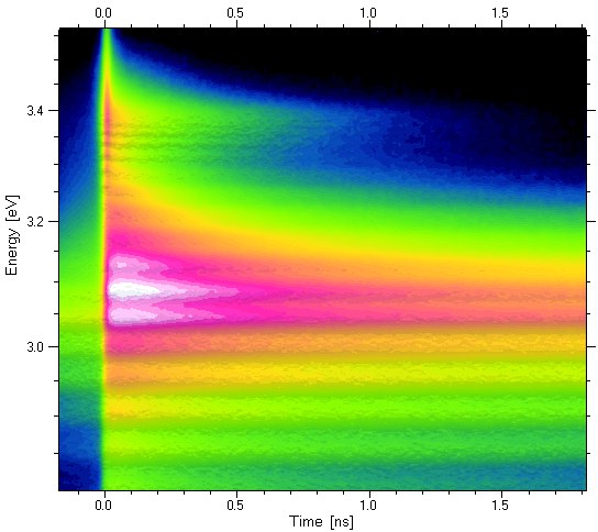 |
TRPL of a GaInN/GaN quantum well on sapphire. GaN barrier emits at about 3.40 eV. The QW PL is at 3.05 eV. The sample was used for investigation of influence of electric fields on optical properties of GaInN/GaN structure. For details see: J. Binder, K. P. Korona, J. Borysiuk, A. Wysmołek, M. Baeumler, K. Köhler, L. Kirste, "Absorption and Emission Properties of Light Emitting Diode Structures Containing GaInN/GaN QWs" , Acta Physica Polonica A 120, p. 918-920 (2011) |
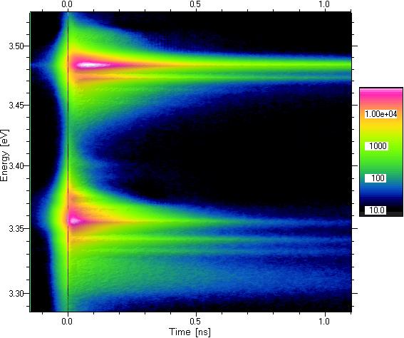 |
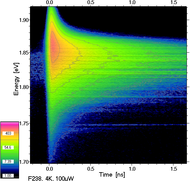
Time-resolved luminescence of zinc oxide (ZnO) grown on gallium nitride (GaN) at 4 K.
ZnO and GaN emit light of energies about 3.36 and 3.48 eV, respectively.
The sample was used for testing of plasmonic coupling to Ag nanoislands. Details in: J. Papierska, B. S. Witkowski, A. Derkachova, K. P. Korona, J. Binder, K. Gałkowski, Ł. Wachnicki, M. Godlewski, T. Dietl, and J. Suffczyński, "Modification of Emission Properties of ZnO Layers due to Plasmonic Near-Field Coupling to Ag Nanoislands" , Plasmonics 8, 913-919 (2013), DOI: 10.1007/s11468-013-9490-5 |
My cooperation with MPI Stutgart was possible due to Alexander von Humbold Fellowship.
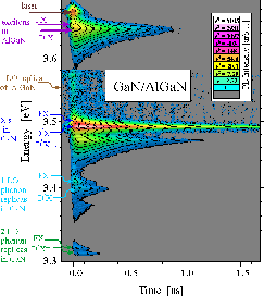 TRPL of a GaN/AlGaN sample. |
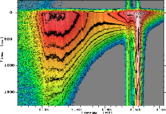 TRPL of a InAs/GaAs structur with quantum dots. |
UV detector containing GaInN QW with AlGaN barriers
(A) Photograph of the sample. (B) Map of intensity of the GaInN QW peak. (C) Map of wavelength of the GaInN QW peak.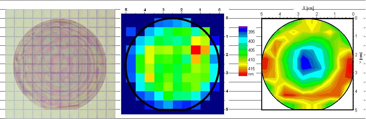
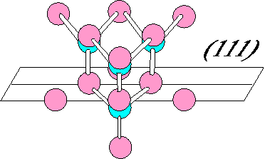
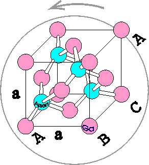
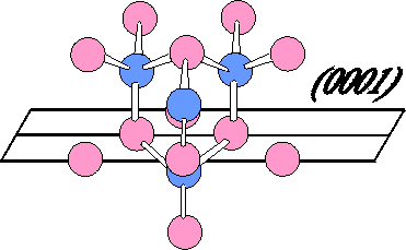
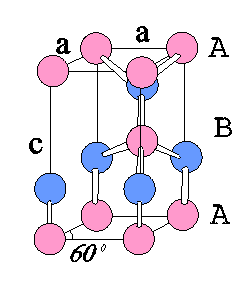
III-V semiconductors
III-V semiconductors are compounds made of elements from third and fifth groups of periodic table of elements. For example, gallium (Ga) from the third group and arsenic (As) from the fifth group form gallium arsenide (GaAs). Well known semiconductor germanium (Ge) is made of atoms from the forth group. If, in Ge crystal, somebody replaces one Ge atom by Ga and next Ge atom by As, will obtain GaAs crystal. Most of III-V and II-VI semiconductors crystallize in zinc-blend (cubic ZnS) or wurtzite (hexagonal ZnS) structures. Typical example of cubic crystal is gallium arsenide, GaAs, lattice (see below). Typical example of hexagonal structure is gallium nitride, GaN (see below).
|
|
|
My WWW page